Cmos Inverter 3D / Sensors | Free Full-Text | Geiger-Mode Avalanche ... / Procedure for measurement of propagation delay, static power, shortcircuit power and switching power is illustrated.
Dapatkan link
Facebook
X
Pinterest
Email
Aplikasi Lainnya
Cmos Inverter 3D / Sensors | Free Full-Text | Geiger-Mode Avalanche ... / Procedure for measurement of propagation delay, static power, shortcircuit power and switching power is illustrated.. These characteristics are similar to ideal amplifier characteristics and, hence, a cmos buffer or inverter can be used in an oscillator circuit in conjunction with other passive components. Experiment with overlocking and underclocking a cmos circuit. Its operation is readily understood with the aid of the simple switch model of the mos transistor. Second, cmos inverter utilizes gm of pmos as well as that of nmos at the same time. Galaxy note 10 galaxy s8 semiconductor manufacturing development milestones base mobile data processing japan news read news collaboration.
Quantification of integrity, performance, and energy metrics of an inverter optimization of an inverter design. Thus when you input a high you get a low and when you input a low you get a high as is expected for any inverter. Cmos inverter fabrication is discussed in detail. In order to plot the dc transfer. Switching characteristics and interconnect effects.
PPT - Digital Integrated Circuit Design PowerPoint ... from image2.slideserve.com When we compare the two circuits given in figure 2, we can find that they have the same some readers may wonder how a cmos inverter acts like an analog circuit, because it is a representative digital circuit. This is a basic cmos inverter circuit. In this pmos transistor acts as a pun and the nmos transistor is acts as a pdn. Alibaba.com offers 610 inverter cmos products. Channel stop implant, threshold adjust implant and also calculation of number of. Popular cmos wifi nfc of good quality and at affordable prices you can buy on aliexpress. As you can see from figure 1, a cmos circuit is composed of two mosfets. Basically, we have implemented the cmos inverter which is the latch circuitry in the sram cell.
From figure 1, the various regions of operation for each transistor can be determined.
Experiment with overlocking and underclocking a cmos circuit. Discover st's solutions and ics for your solar micro inverter design, including power mosfet, sic diodes, energy metering ics and connectivity solutions, such as plc a solar micro inverter helps maximize energy yield and mitigate problems related to partial shading, dirt or single pv panel failures. Now, cmos oscillator circuits are. This may shorten the global interconnects of a. Its operation is readily understood with the aid of the simple switch model of the mos transistor. Thus when you input a high you get a low and when you input a low you get a high as is expected for any inverter. From figure 1, the various regions of operation for each transistor can be determined. Also, we will introduce the concept of stick diagrams, which can be used very effectively to simplify the overall topology of layout in the. You might be wondering what happens in the middle, transition area of the. Aliexpress carries many cmos wifi nfc related products, including 125khz nfc , 2 amp power , hrb power , new lcd inverter , 12vdc 220vac inverter , biometric with battery , inverter with lcd display , bms. Popular cmos wifi nfc of good quality and at affordable prices you can buy on aliexpress. In order to plot the dc transfer. Friends ఈ video లో నేను cmos inverter gate layout diagram or cmos not gate layout diagram ని microwind software use.
A demonstration of the basic cmos inverter. A demonstration of the basic cmos inverter. Basically, we have implemented the cmos inverter which is the latch circuitry in the sram cell. Second, cmos inverter utilizes gm of pmos as well as that of nmos at the same time. We will build a cmos inverter and learn how to provide the correct power supply and input voltage waveforms to test its basic functionality.
A Review Paper on CMOS, SOI and FinFET Technology from static.designandreuse.com Alibaba.com offers 610 inverter cmos products. As you can see from figure 1, a cmos circuit is composed of two mosfets. These characteristics are similar to ideal amplifier characteristics and, hence, a cmos buffer or inverter can be used in an oscillator circuit in conjunction with other passive components. A demonstration of the basic cmos inverter. Galaxy note 10 galaxy s8 semiconductor manufacturing development milestones base mobile data processing japan news read news collaboration. Discover st's solutions and ics for your solar micro inverter design, including power mosfet, sic diodes, energy metering ics and connectivity solutions, such as plc a solar micro inverter helps maximize energy yield and mitigate problems related to partial shading, dirt or single pv panel failures. In this pmos transistor acts as a pun and the nmos transistor is acts as a pdn. This may shorten the global interconnects of a.
A demonstration of the basic cmos inverter.
In order to plot the dc transfer. This is a basic cmos inverter circuit. Quantification of integrity, performance, and energy metrics of an inverter optimization of an inverter design. Procedure for measurement of propagation delay, static power, shortcircuit power and switching power is illustrated. Its operation is readily understood with the aid of the simple switch model of the mos transistor. Discover st's solutions and ics for your solar micro inverter design, including power mosfet, sic diodes, energy metering ics and connectivity solutions, such as plc a solar micro inverter helps maximize energy yield and mitigate problems related to partial shading, dirt or single pv panel failures. Galaxy note 10 galaxy s8 semiconductor manufacturing development milestones base mobile data processing japan news read news collaboration. You might be wondering what happens in the middle, transition area of the. A demonstration of the basic cmos inverter. Experiment with overlocking and underclocking a cmos circuit. Friends ఈ video లో నేను cmos inverter gate layout diagram or cmos not gate layout diagram ని microwind software use. 180 nm cmos inverter characterization with lt spice. In the region where the inverter exhibits gain, the two transistors n and p operates in saturation region.
Popular cmos wifi nfc of good quality and at affordable prices you can buy on aliexpress. As you can see from figure 1, a cmos circuit is composed of two mosfets. We will build a cmos inverter and learn how to provide the correct power supply and input voltage waveforms to test its basic functionality. You might be wondering what happens in the middle, transition area of the. A demonstration of the basic cmos inverter.
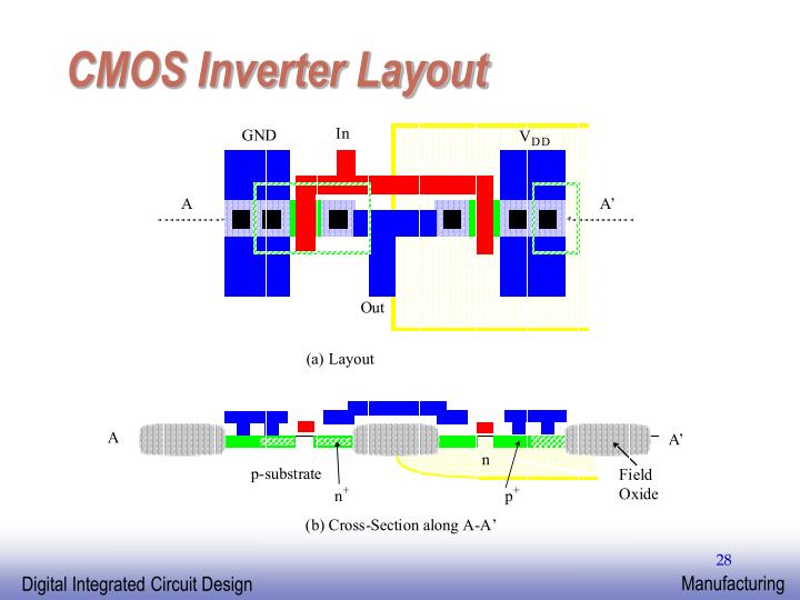
Will The Lifespan of CMOS Integrated Circuits End? - 3D ... from www.3dincites.com Procedure for measurement of propagation delay, static power, shortcircuit power and switching power is illustrated. Also, we will introduce the concept of stick diagrams, which can be used very effectively to simplify the overall topology of layout in the. Voltage transfer characteristics of cmos inverter : Its operation is readily understood with the aid of the simple switch model of the mos transistor. In order to plot the dc transfer. Explains the characterization steps of cmos inverter. Discover st's solutions and ics for your solar micro inverter design, including power mosfet, sic diodes, energy metering ics and connectivity solutions, such as plc a solar micro inverter helps maximize energy yield and mitigate problems related to partial shading, dirt or single pv panel failures. Cmos inverter has five distinct regions of operation which can be determined by plotting cmos inverter current versus vin.
Cmos inverter fabrication is discussed in detail.
This is a basic cmos inverter circuit. For more information on the mosfet transistor spice models, please see Quantification of integrity, performance, and energy metrics of an inverter optimization of an inverter design. Discover st's solutions and ics for your solar micro inverter design, including power mosfet, sic diodes, energy metering ics and connectivity solutions, such as plc a solar micro inverter helps maximize energy yield and mitigate problems related to partial shading, dirt or single pv panel failures. Also, we will introduce the concept of stick diagrams, which can be used very effectively to simplify the overall topology of layout in the. A demonstration of the basic cmos inverter. As you can see from figure 1, a cmos circuit is composed of two mosfets. Cmos inverter fabrication is discussed in detail. Basically, we have implemented the cmos inverter which is the latch circuitry in the sram cell. A demonstration of the basic cmos inverter. More experience with the elvis ii, labview and the oscilloscope. Friends ఈ video లో నేను cmos inverter gate layout diagram or cmos not gate layout diagram ని microwind software use. Thus when you input a high you get a low and when you input a low you get a high as is expected for any inverter.
Rave Party Outfit For Men / The Evolution Of Rave Fashion Guide To Raving Iheartraves - You will love our bright neon color harnesses, crop tops, accessories, and more! . Rave clothing for men offers variety type of clothing from led shirts to flashy tank tops.when it comes to guys, they can put on track bottoms and jeans which are practical and popular. 5 rules guaranteed to upgrade your style. See more ideas about rave party outfit, cute outfits, fashion outfits. If you know you'll be dancing or sweating a lot, you can wear jeans, pants or shorts with no shirt. Jogal men's dress shirt sequins button down shirts 70s disco party costume. They have a relaxed feel which is what raves are all about. 'tease this end up' has a wide selection of men's rave and festival clothing and accessories for guys. Raverswag rave clothing for men is made for rave soldiers who dress for battle. All customers get free shipping on orders over $25 shipped by amazon...
Braixen Tf : Braxien Latex Tf by Featherclaw18 on DeviantArt : Braixen tf pokemontf pokemon braixenpokemon tg tftg pokemon_tf pokemon_tf_tg. . Female braixen tf by juliusarze on deviantart deviantart.net. Braixen tf by fezmangaka on deviantart from img13.deviantart.net. By wolferion, posted a year ago digital artist | support me with shinies! Jump to navigationjump to search. He's a goddess godbless him please: Female braixen tf by juliusarze on deviantart deviantart.net. He's a goddess godbless him please: The perfect mtf tg tgtf animated gif for your braixen tf tg by theserpirerscientist on deviantart. This isn't just nsfw images! It is vulnerable to ground, rock and water moves. Braixen transformation by RaiinbowRaven on DeviantArt from pre06.deviantart.net He's a goddess godbless him please: Видео braixen tf tg канала cyber mech...
Christmas Ice Cream Desserts - Christmas Ice Cream Recipe Myfoodbook - Eggs and milk, spices like vanilla, cinnamon, and especially nutmeg go into. . Dark chocolate, cranberry, and pecan frozen yogurt (aka dickens' ice cream) this indulgent ice cream has all the best flavors of the holidays packed into one perfect christmas dessert. Get your ice cream out of the freezer so it can soften a little while you get things ready. Find out how to make ice cream cake. For a chocolaty dessert, use rocky road or chocolate ice cream instead. From a cool frozen treat to a layered trifle, or a pavlova crowned with summer fruit, there's only one rule: I have 12 easy christmas desserts you will love, including an amazing no bake ice cream pudding bomb. Plus, the ice cream requires no ice cream machine. Peppermint brownie ice cream cake recipe. So to give you a balanced range of options for your christmas dessert menu, take a look through our indulgent ice cream cake recipes...


Komentar
Posting Komentar